| A | B | C | |
| 1 | Reserved | Reserved | PWROFF |
| 2 | Reserved | GND | /NUBUS |
| 3 | /BUSLOCK | /TM1A | /TM0A |
| 4 | /IRQ3 | /IRQ2 | /IRQ1 |
| 5 | /IPL2 | /IPL1 | /IPL0 |
| 6 | /CIOUT | /DS | /RMC |
| 7 | /STERM | /CBACK | /CBREQ |
| 8 | /DSACK1 | /DSACK0 | R/W |
| 9 | SIZ1 | SIZ0 | /AS |
| 10 | /BGACK | /BG | /BR |
| 11 | FC2 | FC1 | FC0 |
| 12 | /RESET | /BERR | /HALT |
| 13 | D0 | +5V | D1 |
| 14 | D2 | D3 | D4 |
| 15 | D5 | D6 | D7 |
| 16 | D8 | GND | D9 |
| 17 | D10 | D11 | D12 |
| 18 | D13 | D14 | D15 |
| 19 | D16 | +5V | D17 |
| 20 | D18 | D19 | D20 |
| 21 | D21 | D22 | D23 |
| 22 | D24 | GND | D25 |
| 23 | D26 | D27 | D28 |
| 24 | D29 | D30 | D31 |
| 25 | A31 | +5V | A30 |
| 26 | A29 | A28 | A27 |
| 27 | A26 | A25 | A24 |
| 28 | A23 | GND | A22 |
| 29 | A21 | A20 | A19 |
| 30 | A18 | A17 | A16 |
| 31 | A15 | +5V | A14 |
| 32 | A13 | A12 | A11 |
| 33 | A10 | A9 | A8 |
| 34 | A7 | GND | A6 |
| 35 | A5 | A4 | A3 |
| 36 | A2 | A1 | A0 |
| 37 | +5V | +5V | +5V |
| 38 | CPUCLOCK | ECLK | C16M |
| 39 | GND | GND | GND |
| 40 | -12V | -5V | +12V |
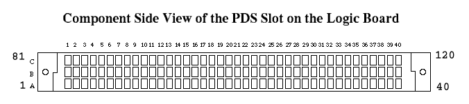
Numbers from 1 to 120 are actually assigned to the PDS slot (EuroDIN connector) pin positions on the logic board circuit.
Four positioning numbers 1, 40, 81 and 120 are printed on the component side of the logic board.
On the rear side of the logic board, mesh patterns indicates the ground (GND) lines.
By comparing the GND pins (B2, B16, B22, B28, B34, A39, B39, C39) with
the mesh patterns, we can determine the correspondence between the
actual pin positions/numbers (1-120) and the assignment numbers (A1-A40,
B1-40, C1-C40) in the above figure.
| A (31-0) | Address lines. |
| FC (2-0) | Function code. |
| D (31-0) | Data lines. |
| /IPL (2-1) | Interrupt priority lines. |
| /CIOUT | Cache inhibit out. |
| /CBREQ | Cache burst request. |
| /CBACK | Cache burst acknowledge. |
| /STERM | Synchronous termination. |
| /DSACK (1-0) | Data acknowledge. |
| /SIZ (1-0) | Transfer size. |
| /BR | Bus request. |
| /BG | Bus grant. |
| /BGACK | Bus grant acknowledge. |
| /RESET | System reset. |
| /BERR | Bus error. |
| /RMC | Read modify cycle. |
| R/W | Read/write. |
| /AS | Address strobe. |
| /HALT | Halt. |
| /DS | Data strobe. |
| PWROFF | Power off. |
| /NUBUS | NuBus space access. |
| /BUSLOCK | NuBus buslock. |
| /TM1A | NuBus transfer mode bit 1. |
| /TM0A | NuBus transfer mode bit 0. |
| /IRQ (3-1) | Interrupt input. |
| CPUCLOCK | 16.67MHz CPU Clock. |
| ECLK | E clock. |
| C16M | 15.6672MHz gen clock. |
| GND | Ground. |